

Chip topography measurement
Measurement requirements
Scanning the three-dimensional topography of the chip surface, extracting the profile and measuring the level difference of the desired position on the surface
Overview of key features
1. Non-contact measurement, integrated design
2. Three-dimensional topography scanning, multi-function data processing
3. Suitable for accurate measurement of various materials
4. Simple to use, easy to assemble and disassemble
5. Fast scanning speed and high positioning accuracy
6.±0.5 to ±1μm repeated accuracy guarantee
7. High stability and strong anti-interference ability
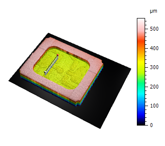
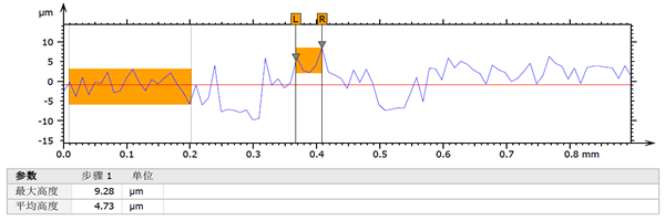
Measurement results
The measured position level difference is about 5μm.
Solve the problems of the current measuring device
1. There are certain requirements for measurement materials
2. Contact measurement, damage to the measurement material
3. The measurement range is small, the position is uncertain, and the measurement is difficult
4. The measurement speed is slow, the precision is low, and the measurement error is large
5. Complex structure and high cost
-
-
-
Customer service contact information
Service hours:9:00 — 18:00
24 hours after sale
Contact number:
-


Hotline:021-37781691
E-Mail:contact@think-focus.com
Address: Room 204, Building D2, Innovation Workshop, No. 6000, Shenzhuan Road, Songjiang District, Shanghai